High-Performance RF Amplifier Design Using the Infineon BFP540 Transistor
The design of radio frequency (RF) amplifiers demands a meticulous balance of gain, linearity, noise performance, and stability. Achieving high performance in applications such as cellular infrastructure, wireless communication systems, and satellite receivers often hinges on the selection of the right active device. The Infineon BFP540, an NPN silicon germanium (SiGe) heterojunction bipolar transistor (HBT), has emerged as a premier choice for low-noise amplification stages in the UHF and microwave bands.
Key Characteristics of the BFP540 Transistor
The BFP540 is engineered for high-frequency performance, offering a compelling set of characteristics that make it ideal for sensitive receiver front-ends. Its low noise figure (NFmin), typically around 0.9 dB at 1.8 GHz, is paramount for preserving the integrity of weak incoming signals. Coupled with high associated gain, this ensures the signal is amplified significantly before the system's inherent noise dominates. Furthermore, the transistor exhibits excellent linearity, characterized by a high output third-order intercept point (OIP3), which is critical for handling strong signals and minimizing intermodulation distortion in crowded spectral environments. Its high transition frequency (fT) of approximately 65 GHz guarantees ample bandwidth for operations well into the S-band.
Critical Design Considerations
A successful amplifier design extends beyond simply selecting a high-performance transistor. Biasing network stability is the foundation of any robust RF design. The operating point (quiescent point) must be chosen carefully to optimize the trade-off between gain, noise figure, and power consumption. A stable DC bias, achieved through resistive networks and decoupling capacitors, is essential to prevent performance drift and oscillations.
Impedance matching is arguably the most critical step in realizing the device's potential. For a low-noise amplifier (LNA), the input network is not matched for maximum power transfer (conjugate match) but for the minimum noise figure, a condition specified by the optimum source reflection coefficient (Γopt) provided in the device's datasheet. This noise matching strategy often sacrifices a small amount of gain for a vastly superior noise performance. The output network, however, is typically matched for maximum gain and power transfer to the subsequent stage.
Stability analysis must be performed across the entire frequency band of operation, not just the center frequency. A transistor can be potentially unstable at certain frequencies, leading to unwanted oscillations. Employing techniques such as stabilization resistors or negative feedback ensures unconditional stability across a wide spectrum, making the design reliable and manufacturable. Simulating the Rollett stability factor (K-factor) is a standard practice to verify this.

Implementation and Layout
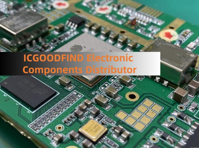
Practical implementation requires a high-quality printed circuit board (PCB) with a well-designed RF ground plane. The use of microstrip transmission lines for matching networks is standard. Surface-mount technology (SMT) components must be used to minimize parasitic inductance and capacitance. The physical layout is critical; keeping input and output traces separated, using ample vias for grounding, and shielding sensitive nodes are all necessary to prevent feedback and oscillation. Simulations using tools like ADS or Microwave Office are indispensable for optimizing the design before fabrication.
ICGOOODFIND
This article underscores that designing a high-performance RF amplifier with the Infineon BFP540 is a systematic process that leverages the transistor's superior low-noise and high-frequency capabilities. Success is achieved through rigorous attention to biasing stability, precise noise-matched input networks, and ensuring unconditional stability across all frequencies. A robust PCB layout completes the transition from theoretical design to a practical, high-gain, and low-noise amplifier stage.
Keywords:
1. Low-Noise Amplifier (LNA)
2. Impedance Matching
3. Noise Figure
4. Stability Analysis
5. Silicon Germanium (SiGe)
